


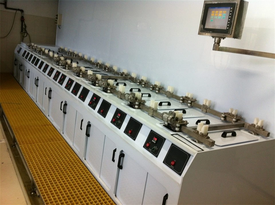


Electroless Copper Plating Equipment
Electroless Copper Plating Equipment (JYC-ELC-Series)
Built for PCB Through-Hole Metallization and Plating on Plastics
PCB through-hole walls, plastic parts for plating, and decorative coatings. These applications need a conductive layer before electroplating. Our Electroless Copper Plating Equipment provides this. The process deposits a thin copper layer without electric current. Thickness is typically 0.5 to 1.5 microns for PCB applications. For plastic parts, thickness ranges from 1 to 3 microns. The copper layer is dense and uniform. It provides excellent adhesion to both hole walls and plastic surfaces. This process is the foundation for all subsequent electrolytic copper plating. It meets IPC-6012 for PCB manufacturing. Our SAP electroless copper line for the Beijing Microelectronics Institute was 10 years ahead of domestic peers.

Materials and Construction for Chemical Stability

The electroless copper bath is sensitive to contamination. We use high-purity PP tanks and corrosion-resistant pumps. Temperature is controlled at 30 to 45°C depending on the bath formulation. Filtration is continuous at 1-micron precision. We include automatic replenishment for copper salt, reducing agent, and stabilizers. Online monitors track copper concentration, pH, and specific gravity. The system adjusts dosing automatically to maintain stable deposition rates.
Three Core Advantages
First, hole wall coverage is complete.
Our bath chemistry has excellent throwing power. Even in high-aspect-ratio holes, the copper layer covers the entire hole wall. There are no voids or discontinuities. This ensures reliable electrical connections.
Second, adhesion to plastics is strong.
For plastic plating applications, the electroless copper layer bonds well with the etched plastic surface. Peel strength exceeds 1.5 N/cm. This is verified by ASTM B533 testing.
Third, bath stability is exceptional.
Our stabilizer system prevents spontaneous decomposition of the bath. Bath life extends beyond 6 months with proper maintenance. Operating costs are lower.
What Buyers Often Ask
Buyers ask us: "PCB customers need consistent hole wall coverage. How do you ensure it?" We provide automatic analysis and replenishment. Bath composition stays within tight tolerances. Coupon testing and cross-section analysis verify hole wall coverage in real time. Our electroless copper lines have been proven in high-volume PCB production for many years.
Technical Specifications
|
Parameter |
Specification |
|
Copper Layer Thickness (PCB) |
0.5 – 1.5 µm |
|
Copper Layer Thickness (Plastics) |
1 – 3 µm |
|
Bath Temperature |
30 – 45°C |
|
Filtration Precision |
1 µm |
|
Adhesion to Plastic |
≥ 1.5 N/cm |
|
Applicable Standards |
IPC-6012, ASTM B533 |
Hot Tags: electroless copper plating equipment, China electroless copper plating equipment manufacturers, suppliers, factory, Al Mg Passivation Equipment, El Ni Pd Au Equipment, Electroless Copper Plating Equipment, Electropolishing Equipment, Phosphating Equipment, surface treatment equipment
Previous
El Ni-Pd-Au EquipmentYou Might Also Like


Send Inquiry